Quantum sensors in semiconductor manufacturing

Inefficient quality control process exacerbating chip shortages
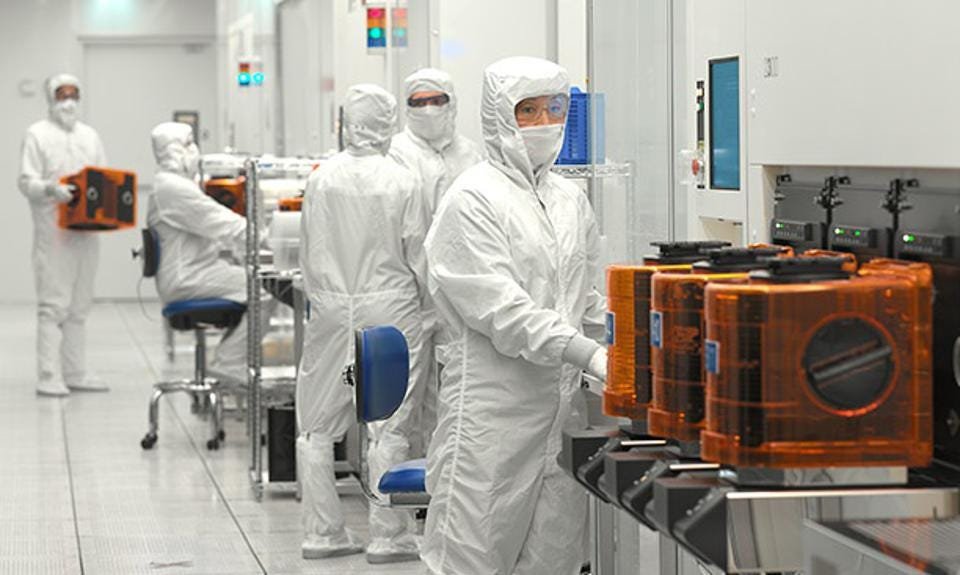
Semiconductor manufacturing is high-end - being both capital-heavy and technologically intensive. They are essential in devices needing computing power, having high demand but with very limited foundries producing them. Last year, the US government approved $52 billion for domestic semiconductor manufacturing. Across the Atlantic, a new factory was opened in Germany, with Bosch making a huge investment in opening a $1.2 billion chip plant for electric vehicles. These chips begin with thin silicon wafers, which are then printed with complex electronics and cut into individual circuits. As they get smaller and smaller, the quality control process (i.e. checking for current leakages) is getting more and more challenging. QuantumDiamonds had discussions with the industry and learned about the quality assurance process, which is where quantum sensing with its high sensitivity and spatial resolution is a natural fit for. A human, using optical scanning (optical beam induced resistance change) or imaging technology (lock-in thermography), reviews each circuit or the wafer as a whole to check for issues. Both techniques are slow and depend on the chip being infrared transparent. The flawed product can then be removed, and then the stamps or design can be reviewed for faults. Manufacturers are having a difficult time meeting quality assurance standards. This results in a costly and inefficient manufacturing process with up to 20% scrapping rate costing a single plant 87.5 to 140 million dollars a year in losses. Moreover, these losses exacerbate supply shortages.
Quantum sensors as a solution
Current through an integrated circuit (IC) or a print circuit board generates a small vector magnetic field. Researchers at the University of Maryland used a quantum diamond microscope to measure simultaneously all three components (x y and z) of a magnetic field across a 4 x 4 mm² field of view with 1 µm lateral spatial resolution. On the 8 nm process node flip chip IC, the magnetic field from a collapsed connection (C4 bump) was the most salient feature. The authors used it in image registration while image processing. In addition, they subtracted it and were able to distinguish nearby current traces on the micron scale. They were also able to see the 3D current distribution on a multi-layer PCB. A current was detected both along a 200 µm vertical via. After mathematical processing, the current density from three unique active layers was isolated. The separation between the two conducting layers was also verified. These results combined with AI and improvements to the technique’s spatial resolution would make it a valuable tool for quality control in semiconductor manufacturing.
To understand more about the use cases for quantum sensing technology in semiconductor manufacturing, reach out to our technology specialist Fleming Bruckmaier!
Read publications: